- 您现在的位置:买卖IC网 > Sheet目录3841 > DSPIC30F1010-30I/SP (Microchip Technology)IC DSPIC MCU/DSP 6K 28DIP
2010 Microchip Technology Inc.
DS70102K-page 51
dsPIC30F Flash Programming Specification
11.11 Reading Configuration Memory
The procedure for reading configuration memory is
similar to the procedure for reading code memory,
except that 16-bit data words are read instead of 24-bit
words. Since there are seven Configuration registers,
they are read one register at a time.
Table 11-11 shows the ICSP programming details for
reading all of the configuration memory. Note that the
TBLPAG register is hard-coded to 0xF8 (the upper byte
address of configuration memory), and the read pointer
W6 is initialized to 0x0000.
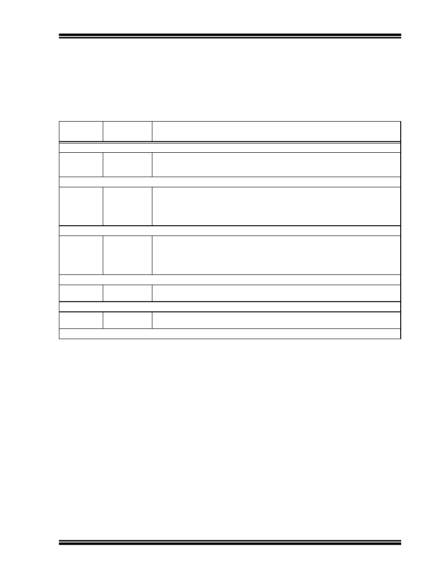
TABLE 11-11: SERIAL INSTRUCTION EXECUTION FOR READING ALL CONFIGURATION MEMORY
Command
(Binary)
Data
(Hexadecimal)
Description
Step 1: Exit the Reset vector.
0000
040100
000000
GOTO 0x100
NOP
Step 2: Initialize TBLPAG, and the read pointer (W6) and the write pointer (W7) for TBLRD instruction.
0000
200F80
880190
EB0300
EB0380
000000
MOV
#0xF8, W0
MOV
W0, TBLPAG
CLR
W6
CLR
W7
NOP
Step 3: Read the Configuration register and write it to the VISI register (located at 0x784).
0000
BA0BB6
000000
883C20
000000
TBLRDL [W6++], [W7]
NOP
MOV
W0, VISI
NOP
Step 4: Output the VISI register using the REGOUT command.
0001
0000
<VISI>
000000
Clock out contents of VISI register
NOP
Step 5: Reset device internal PC.
0000
040100
000000
GOTO 0x100
NOP
Step 6: Repeat steps 3-5 six times to read all of configuration memory.
发布紧急采购,3分钟左右您将得到回复。
相关PDF资料
PIC24FJ64GB002-I/ML
IC MCU 16BIT 64KB FLASH 28QFN
52746-1270
CONN FFC 12POS .5MM R/A ZIF SMD
TS80C31X2-MCE
IC MCU 8BIT 40/20MHZ 44-VQFP
52746-0870
CONN FFC 8POS .5MM R/A ZIF SMD
PIC24FJ128GA008-I/PT
IC PIC MCU FLASH 128K 80TQFP
PIC16F737-I/SP
IC PIC MCU FLASH 4KX14 28DIP
PIC18F86K22-I/PTRSL
MCU PIC 64K FLASH XLP 80TQFP
PIC16C63A-04I/SP
IC MCU OTP 4KX14 PWM 28DIP
相关代理商/技术参数
DSPIC30F1010-30I/W
制造商:MICROCHIP 制造商全称:Microchip Technology 功能描述:28/44-Pin High-Performance Switch Mode Power Supply Digital Signal Controllers
DSPIC30F1010AT-20E/PF
制造商:MICROCHIP 制造商全称:Microchip Technology 功能描述:High-Performance, 16-Bit Digital Signal Controllers
DSPIC30F1010AT-20I/PF
制造商:MICROCHIP 制造商全称:Microchip Technology 功能描述:High-Performance, 16-Bit Digital Signal Controllers
DSPIC30F1010AT-30I/PF
制造商:MICROCHIP 制造商全称:Microchip Technology 功能描述:High-Performance, 16-Bit Digital Signal Controllers
DSPIC30F1010BT-20I/PF
制造商:MICROCHIP 制造商全称:Microchip Technology 功能描述:High-Performance, 16-Bit Digital Signal Controllers
DSPIC30F1010BT-30I/PF
制造商:MICROCHIP 制造商全称:Microchip Technology 功能描述:High-Performance, 16-Bit Digital Signal Controllers
DSPIC30F1010CT-20I/PF
制造商:MICROCHIP 制造商全称:Microchip Technology 功能描述:High-Performance, 16-Bit Digital Signal Controllers
DSPIC30F1010CT-30I/PF
制造商:MICROCHIP 制造商全称:Microchip Technology 功能描述:High-Performance, 16-Bit Digital Signal Controllers